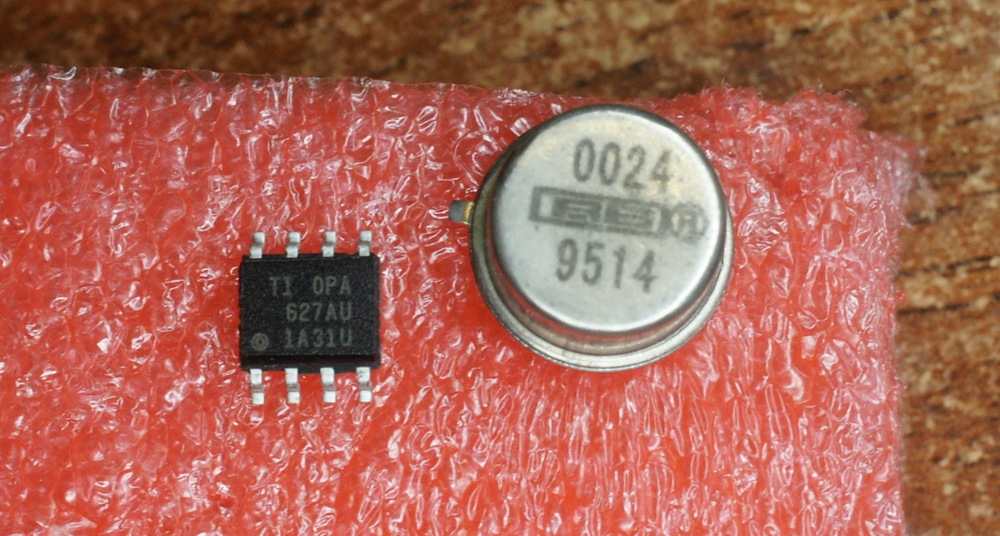
↧
TI LM393 - dual comparator : weekend die-shot
↧
TI TL431 adjustable shunt regulator : weekend die-shot
↧
↧
SiTime SiT8008 - MEMS oscillator : weekend die-shot

Photo of MEMS die puzzled us for quite some time. Is it some sort of integrated SAW/STW resonator?
The trick is that to reach maximum Q-factor (up to ~186'000 according to patents) MEMS resonator must operate in vacuum. So they package resonator _inside_ the die in hydrogen atmosphere, then anneal it in vacuum so that hydrogen escapes through silicon. So we see here only a cap with contacts to "buried" MEMS resonator. We were unable to reach the resonator itself without x-ray camera or ion mill.
MEMS die size - 457x454 µm.
Thankfully relevant patents were specified right on the die : US6936491 US7514283 US7075160 US7750758 :)

Digital die contains LC PLL and digital logic for one-off frequency programming and temperature compensation.
Die size - 1409x1572 µm.

Poly level:

Standard cells ~250nm techology.

↧
Fake audiophile opamps: OPA627 (AD744?!)

Obviously, something fishy was going on. I ordered one, and for comparison - older one in metal can package, apparently desoldered from some equipment. Let's see if there is any difference.

Plastic one was dissolved in acid, metal can was easily cut:

Comparison
Genuine TI/BB OPA627 chip first. We can see here at least 4 laser-trimmed resistors - now we see why it could cost that much. Laser trimmed resistors are needed here due to unavoidable manufacturing variation - parts inside opamps needs to be balanced perfectly.
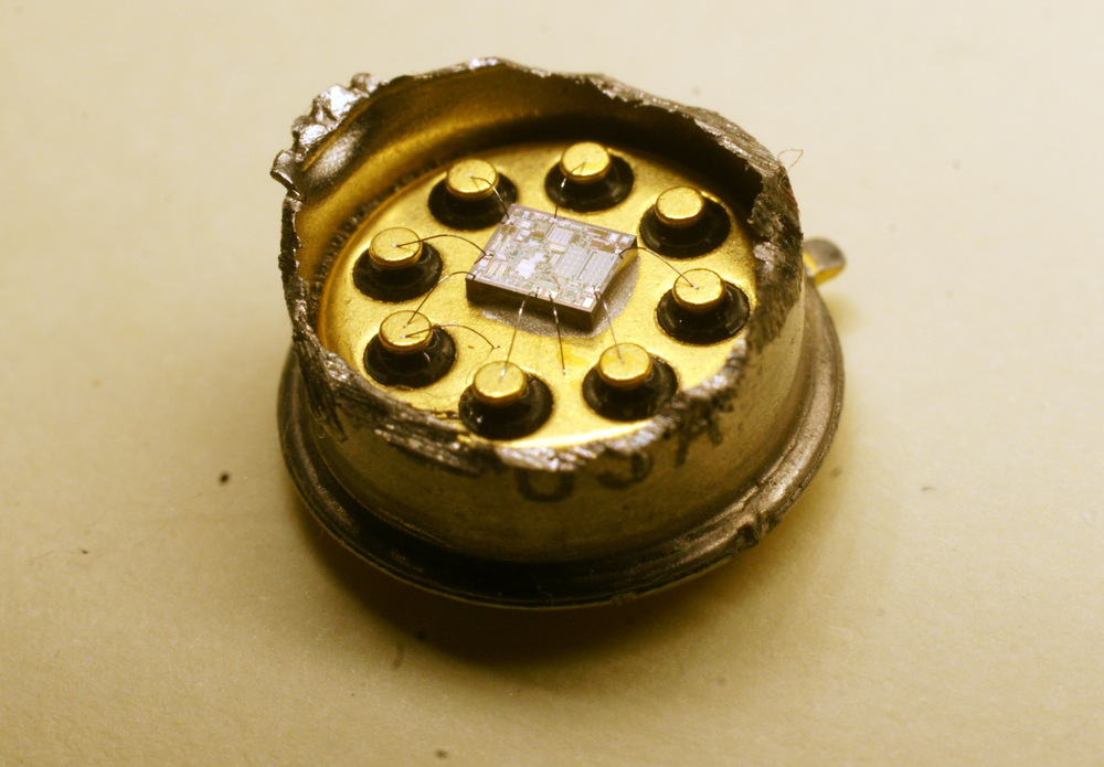
"Chinese" 2.7$ chip. There is only 1 laser trimmed resistor, but we also notice markings AD (Analog Devices?) and B744. Is it really AD744? If we check datasheet на AD744 - we'll see that metal photo perfectly matches one in the datasheet .

What happened here?
Some manufacturer in China put an effort to find cheaper substitute for OPA627 - it appeared to be AD744. AD744 has similar speed (500ns to 0.01%), similar type (*FET), supports external offset compensation. AD744 also support external frequency compensation (for high-speed high-gain applications) but there was no corresponding pin on the OPA627 - so this feature is unused.On the other hand AD744 has higher noise (3x) and higher offset voltage (0.5mV vs 0.1mV).
So they bought AD744 in the form of dies or wafers, packaged them and marked as OPA627. It does not seems they earned alot of money here - it's more of an economic sabotage. Good thing that they did not used something like LM358 - in that case it would have been much easier to notice the difference without looking inside...
Be careful when choosing suppliers - otherwise your design might get "cost-optimized" for you :-)
PS. Take a look at our previous story about fake FT232RL.
↧
Phillips PCF8574 - 8-bit I2C port expander : weekend die-shot
↧
↧
SkyWorks AAT4292 - 7-bit high-side IO expander: weekend die-shot
↧
Toshiba TCD1201D - linear CCD : weekend die-shot
Toshiba TCD1201D is a monochrome 2048-pixel linear CCD. You can also notice few extra pixels for calibration shielded with aluminum.
Die size 34814x802 µm.
![]()
With this die we've reached JPEG limits, full image would be 80k+ pixels wide, so we'll show beginning and the end of the CCD separately:
![]()
![]()
We are grateful to Kony for this chip.
Die size 34814x802 µm.

With this die we've reached JPEG limits, full image would be 80k+ pixels wide, so we'll show beginning and the end of the CCD separately:


We are grateful to Kony for this chip.
↧
KR580VM80A - getting ready for reverse engineering : weekend die-shot
We decided to take a closer look at the most popular soviet processor KR580VM80A (first shoot), so that group of enthusiasts (russian only) would be able to recover schematic from it's layout.
![]()
A bit more dirt, but less overetch:
![]()
Dark field - metal is clearly visible:
![]()
Polarized light - metal and vias are visible:
![]()
After metallization etch. Any ideas why polysilicon gone?
![]()

A bit more dirt, but less overetch:

Dark field - metal is clearly visible:

Polarized light - metal and vias are visible:

After metallization etch. Any ideas why polysilicon gone?

↧
Milandr 1986VE21 : weekend die-shot
↧
↧
OPA627, genuine one this time : weekend die-shot
Last time we decapped 2 fake OPA627's from ebay: one was remarked AD744 part, another was unidentified remarked BB part.
Recently reader sent us one more OPA627 from ebay. This chip appeared to be genuine.
Die size 2940x2005 µm.
![]()
Recently reader sent us one more OPA627 from ebay. This chip appeared to be genuine.
Die size 2940x2005 µm.

↧
KILAR KV1084 5A linear regulator : weekend die-shot
Remember good old times when you could feed CPU from single linear regulator? KILAR KV1084 came from this time.
Comparing to LM2940L or LM1117 there are more bonding pads per signal and obviously larger output transistors. Chip was soldered on copper heat spreader to help dissipate 10W+.
Die size 3075x3026 µm.
![]()
Comparing to LM2940L or LM1117 there are more bonding pads per signal and obviously larger output transistors. Chip was soldered on copper heat spreader to help dissipate 10W+.
Die size 3075x3026 µm.

↧
NXP PCA9570 - 4-bit IO expander : weekend die-shot
↧
Fairchild NC7SZ57 - universal 2-input gate : weekend die-shot
Fairchild NC7SZ57 (and 58) - are universal 2-input shmitt gates, which let us implement various 2-input logic functions by wiring pins in different ways.
Die size 416x362 µm, which is the smallest among microchips we've seen.
Comparing to 1-gate NAND2 Ti SN74AHC1G00 - die area here is 1/3 smaller because area below pads is not wasted and used for IO transistors and wiring. It is unclear though how they achieved decent yields (as things there might get damaged during wire bonding) - we can only tell that insulation before last metal is much thicker than usual.
Drop us a message if you have experience or knowledge on getting high-yield logic under pads - this is something we would be interested to have in our own product.
![]()
Die size 416x362 µm, which is the smallest among microchips we've seen.
Comparing to 1-gate NAND2 Ti SN74AHC1G00 - die area here is 1/3 smaller because area below pads is not wasted and used for IO transistors and wiring. It is unclear though how they achieved decent yields (as things there might get damaged during wire bonding) - we can only tell that insulation before last metal is much thicker than usual.
Drop us a message if you have experience or knowledge on getting high-yield logic under pads - this is something we would be interested to have in our own product.

↧
↧
Ti CC1100 (formerly Chipcon) : weekend die-shot
Ti CC1100 is a radio transceiver for 300-348 MHz, 400-464 MHz and 800-928 MHz ranges.
![]()
Apparently there are 30 initials of the people, involved in the design of this chip mentioned at the lower right corner. Although this chip was designed after Ti acquisition of Chipcon (that happened in January 2006), it is still marked as Chipcon.

Apparently there are 30 initials of the people, involved in the design of this chip mentioned at the lower right corner. Although this chip was designed after Ti acquisition of Chipcon (that happened in January 2006), it is still marked as Chipcon.

↧
Atmel AT90USB162 : weekend die-shot
↧
74HC4094 - 8-bit shift register : weekend die-shot
↧
Analog Devices AD558 - MIL-Spec 8-bit I²L DAC : weekend die-shot
Analog Devices AD558 is an 8-bit I²L DAC in ceramic package (MIL spec).
It is still an open question how this chip got into ex-USSR/Russia - anonymous reader left no comments on that (this smells like cold war...). It is not a secret that Russia had no extensive civilian IC assortment in manufacturing, hence all military IC's must have been designed and manufactured from scratch (i.e. all R&D, prototypes and masks must be paid by government). In such conditions providing all variety of domestic ICs is economically impossible, at least without government expenses comparable to whole world's expenses on IC R&D. So "temporary", "case-by-case" permit to use imported (both legitimately and not-so-legitimately) western ICs in military equipment "until domestic products are ready" is still here after 24 years despite numerous attempts to end this practice.
Die size 2713x2141 µm, 6µm manufacturing technology, trimming laser was leaving ~8µm diameter spots.
![]()
Oh, these rounded resistors are just beautiful... Autorouters in 2014, do you see this?
Note how amount of laser trimming on R-ladder is different for different bits.
![]()
PS. Could anyone share position of western engineers on plastic-vs-ceramic package for military/space-grade IC's? It appears modern plastic packages offer more benefits (like better G-shock/vibration reliability and obviously cost) without sacrificing anything (temperature range and moisture are less of a concern now, radiation was never a concern for a package).
It is still an open question how this chip got into ex-USSR/Russia - anonymous reader left no comments on that (this smells like cold war...). It is not a secret that Russia had no extensive civilian IC assortment in manufacturing, hence all military IC's must have been designed and manufactured from scratch (i.e. all R&D, prototypes and masks must be paid by government). In such conditions providing all variety of domestic ICs is economically impossible, at least without government expenses comparable to whole world's expenses on IC R&D. So "temporary", "case-by-case" permit to use imported (both legitimately and not-so-legitimately) western ICs in military equipment "until domestic products are ready" is still here after 24 years despite numerous attempts to end this practice.
Die size 2713x2141 µm, 6µm manufacturing technology, trimming laser was leaving ~8µm diameter spots.

Oh, these rounded resistors are just beautiful... Autorouters in 2014, do you see this?
Note how amount of laser trimming on R-ladder is different for different bits.

PS. Could anyone share position of western engineers on plastic-vs-ceramic package for military/space-grade IC's? It appears modern plastic packages offer more benefits (like better G-shock/vibration reliability and obviously cost) without sacrificing anything (temperature range and moisture are less of a concern now, radiation was never a concern for a package).
↧
↧
Espressif ESP8266 WiFi-serial interface : weekend die-shot
Since August of 2014 internet is literally blown by WiFi-serial modules on new ESP8266 chip which are currently being sold for less than 4$. Chinese company Espressif managed to cram entire WiFi, TCP/IP and HTTP stack into on-chip memory, without external DRAM. Analog front-end requires minimal external components, all filters are internal. All this allowed them to offer extremely aggressive price. Chip has marking ESP8089, which is their more advanced 40nm product. Apparently, they only differ in bonding and ROM content.
Die size 2050x2169 µm, half of which is occupied by transceiver and PA, 25% - on-chip memory (rough size estimations are ~300KiB), and the rest is Xtensa LX106 CPU core and other digital logic.
![]()
![]()
Chinese engineers did an outstanding job here on finally making WiFi IoT devices cost effective. Let's hope Espressif will eventually open more internal chip information for amateurs and end users.
Die size 2050x2169 µm, half of which is occupied by transceiver and PA, 25% - on-chip memory (rough size estimations are ~300KiB), and the rest is Xtensa LX106 CPU core and other digital logic.


Chinese engineers did an outstanding job here on finally making WiFi IoT devices cost effective. Let's hope Espressif will eventually open more internal chip information for amateurs and end users.
↧
NXP 2N7002 N-channel MOSFET : weekend die-shot
↧
OnSemi MMBT2222A - npn BJT transistor : weekend die-shot

Die size 343x343 µm. Comparing to NXP BC847B die area is 1.5 larger (0.118 vs 0.076mm²), but maximum continuous collector current is 6 times higher (600mA vs 100mA, SOT-23 in both cases). This huge increase in current per transistor area is achieved by shunting thin (=high-resistance) base layer with metal. High resistance of base layer is the limiting factor for maximum collector current in BC847B.
↧